SAM-Based Molecular Junction Devices
A simple, inexpensive and rapid prototyping method to construct thin film molecular spintronic devices has been developed. The goal is to study the spin-polarized current tunneling through a self-assembled monolayer (SAM) spacer. This unique multilayer device provides an excellent test bed to investigating the spintronic behavior at the molecular level. It is of great significance for fundamental understandings of ballistic electron transport through nanoscale thickness molecular monolayers. Metal/SAM/metal junction array can be established via contact printing, a promising way to hybridize an inorganic metal layer onto an organic molecular layer without degrading the organic molecules. Magnetoresistance effects will be examined under external applied magnetic fields and variable temperatures.
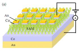
Molecule and magnetic metal-based sandwich junctions can be used for molecular memory and magnetic tunneling junction data storage. For example, a sandwich structure consisting of Au/Co/SAM/Co/Au is displayed in the Figure 2. The reactive layer is an alkanedithiol with the functional group SH at both ends of the molecule. The bottom double layer was deposited on Si with a very thin underlying Ti adhesion layer (2-5 nm) by e-beam evaporation. The coated substrate was immersed into a dilute alkanedithiol solution for 24 hours. Molecules close packed themselves into a self-assembled monolayer on metal Co thin film. The other head groups of the molecules are now facing out and ready to bond to another layer of metal. The top double-layer metal array can be transferred onto the SAM from a pre-coated elastomeric PDMS stamp with desired features. Various metals and molecules may be incorporated in different combinations to support interesting applications such as chemical sensors and biomaterial detectors.

Figure 2. (a) Schematic of the molecular sandwich array and the two-terminal electrical transport circuit. (b) Micrograph of an Au/Co/SAM/Co/Au junction array. Dark green areas are printed metal bilayer; light circular areas around the square features are areas where no printing occurred due to the stamp deformation during contact.

